


SKU/Artículo: AMZ-B0D2QPT7BT
Esthepro
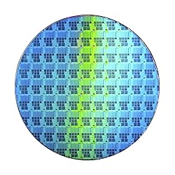
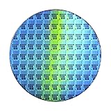
Esthepro Integrated Circuits Silicon Wafer Made by Copper Process (8 Inch)
Size:
8 Inch
Detalles del producto
Disponibilidad:
En stock
En stock
Peso con empaque:
0.15 kg
0.15 kg
Devolución:
Sí
Sí
Condición
Nuevo
Nuevo
Producto de:
Amazon
Amazon
Viaja desde
USA
USA
Sobre este producto
- Semiconductors or chips are produced from silicon. The silicon wafers are etched with millions of tiny transistors 100 times smaller than a human hair. These semiconductors manage data by controlling the flow of electrical current to make words, numbers, sounds, images and colors. They are used worldwide by all major integrated circuit manufacturers and indirectly by nearly every human on the planet. Applications can be found in commonplace items like computers, telecommunications and televisions, as well as in more advanced applications like microwave transmissions, laser switching systems, medical diagnostic and treatment equipment. This one is in excellent shape with no cracks that we could see. 90~130nm minimum microchip feature Copper Characterization with TEOS or Black Diamond Low-k ILD on the single crystal silicon wafer. It has been optically polished till ILD layer and showed blue or green background depend on the ILD material and thickness. Beautiful microchip pattern structure made by the advanced copper technology The original value of un-polished wafer is above $500 Great to be used as gift, display object, exhibition, educating demonstration, testing, decoration or your collection. No guarantee for research and other applications. WARNING! The Wafer is very fragile, a broken wafer can be dangerous due to the sharp edges can cause injuries. Consider it as thin glassware, handle and display it with care. Keep away to the children. We will pack it very well for transport.
AR$102.518
31% OFF
AR$70.697
IMPORT EASILY
By purchasing this product you can deduct VAT with your RUT number
AR$102.518
31% OFF
AR$70.697
con envío
Este producto viaja
de USA ![]() a tus manos en
a tus manos en
![]()
Conoce más detalles
Wafer Pattern May Vary from the Product Images. Great to be used as gift, display object, exhibition, educating demonstration, testing, decoration or your collection Beautiful microchip pattern structure made by the advanced copper technology 90~130nm minimum microchip feature Copper Characterization with TEOS or Black Diamond Low-k ILD on the single crystal silicon wafer The original value of un-polished wafer is above $500 No guarantee for research and other applications
Compra protegida
Disfruta de una experiencia de compra segura y confiable
Tarjetas de Crédito y Débito
Visa
Mastercard
American Express
Pagos a través de PayPal
Compra procesada en dólares con dinero en cuenta o tarjetas internacionales.
Paypal
Pagos a través de MODO
Compra procesada en pesos desde la App de tu banco.
PayPal